Back
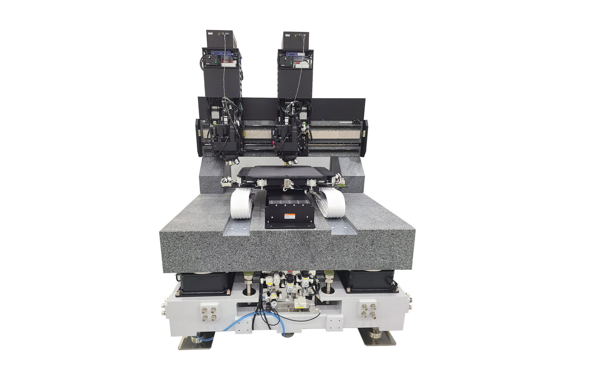
3D Nano Scan Inspection System
3D surface topography measurement using the principle of white light interferometry – step height and CD measurement of microscopic patterns
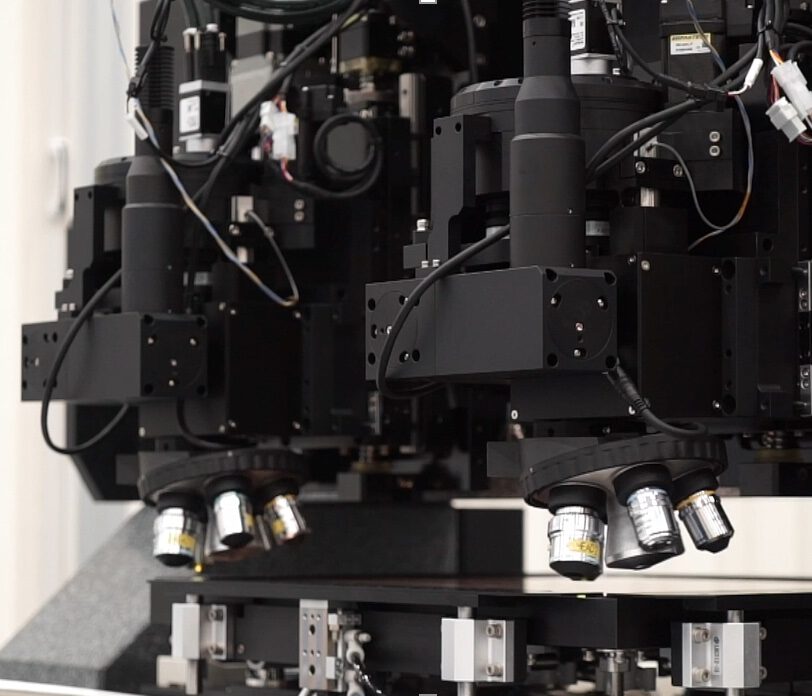
Multi Head
1~16 (EA)
Substrate Compatibility
100~3000 (mm)

High technology
- Non-contact 3D surface profilometry
- Sub-nanometer vertical resolution, high-speed measurement
- Multi-head and composite head configuration (3D Profiler & IR Thickness Measurement & Confocal Head & Contact Thickness Measurement)

Application
- Plating, circuitry, and PSR processes of PS substrates (FC BGA/FC CSP), MLB, and PLP