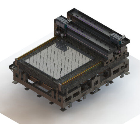
Inspection Equipment
Auto Vision Inspection System
Surface defect inspection equipment for PCB manufacturing processes (surface inspection / SR and gold plating inspection)
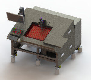
Inspection Equipment
Dual Verification Review System
Equipment for capturing specific images by receiving the coordinates of substrate defect locations identified by AOI
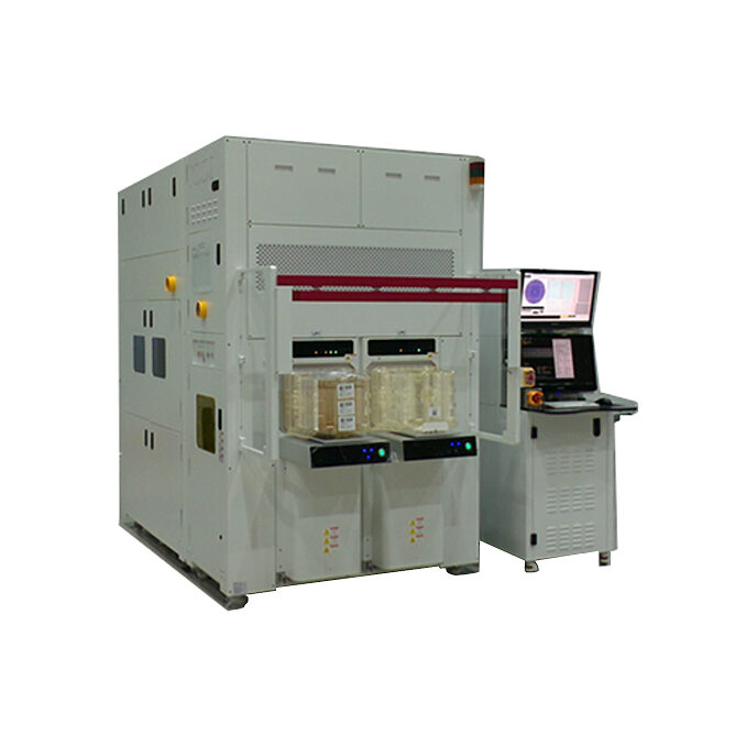
Measurement Equipment
3D Bump Inspection System
3D surface measurement equipment using the principle of white light interferometry
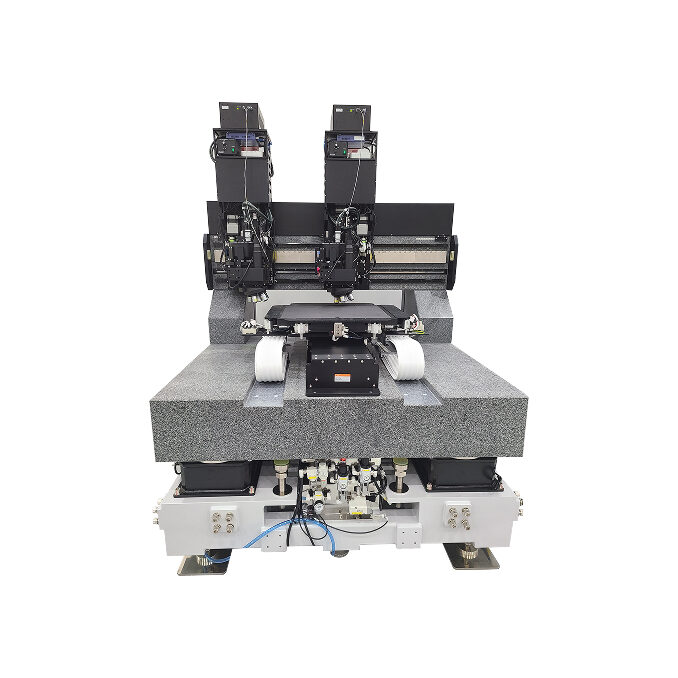
Measurement Equipment
3D Nano Scan Inspection System
3D surface topography measurement using the principle of white light interferometry – step height and CD measurement of microscopic patterns