Back
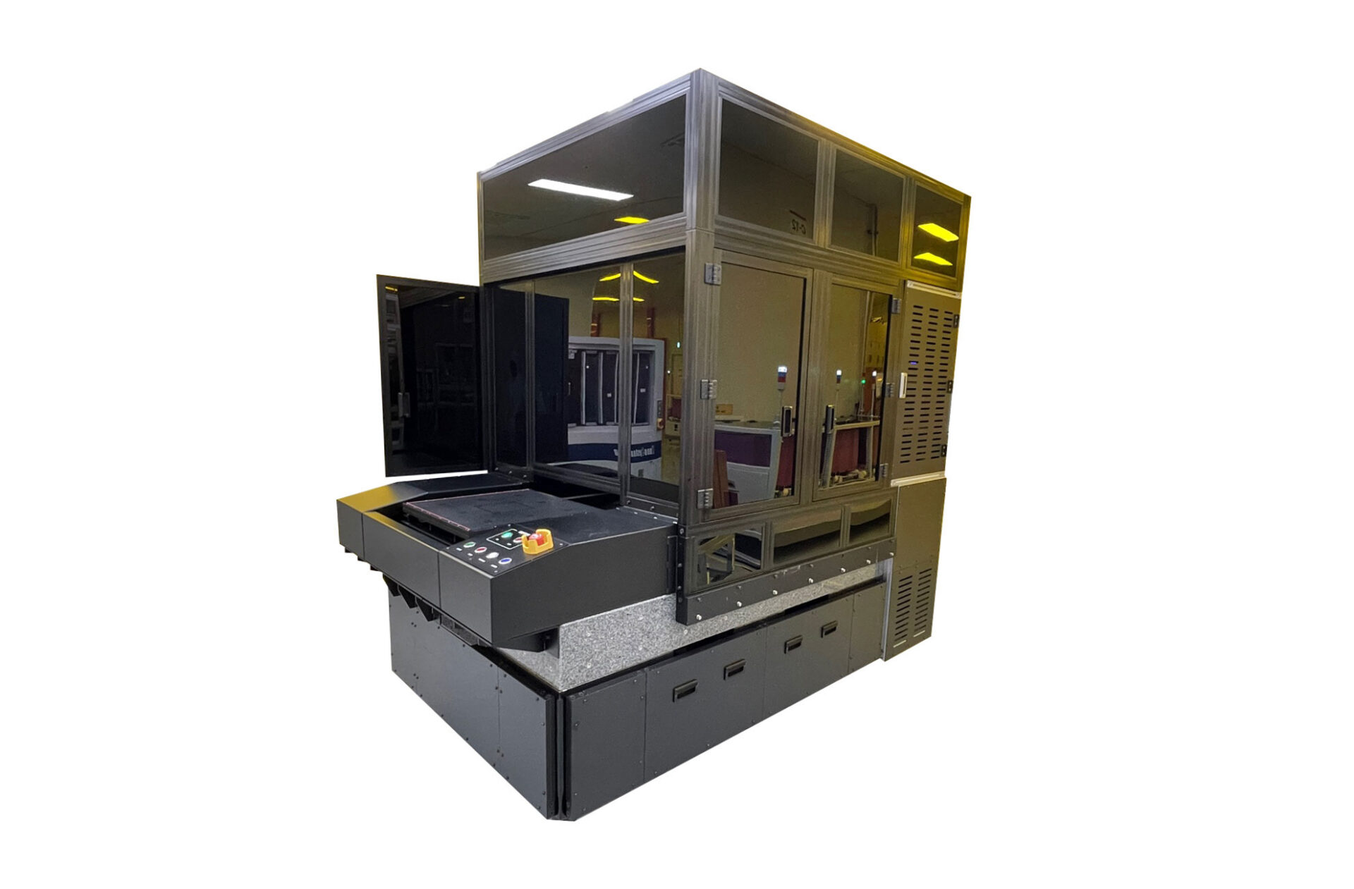
Auto Vision Inspection System
Surface defect inspection equipment for PCB manufacturing processes (surface inspection / SR and gold plating inspection)
PSR & gold-plating surface inspection capability
Sub-PSR pattern inspection capability (multi-spectral illumination technology)

High technology
- PSR and simultaneous gold plating inspection with multi-head technology
- PSR lower pattern inspection available (complex lighting technology)

Application
- PSR process of PCB substrate: Open, Uneven, Cu/Au Exposure, Undercut, SR Discolor, undeveloped PSR, delamination, etc)
- Gold plating process on PCB substrates: layer plating, plating stain, Ni non-plating, white plating, discoloration, Ni agglomeration, Ni exposure, etc