Back
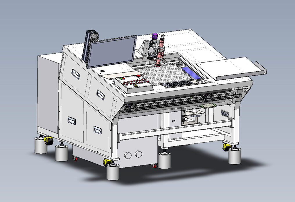
Dual Verification Review System
Equipment for capturing specific images by receiving the coordinates of substrate defect locations identified by AOI
Capable of verifying fine line widths
Provide high-resolution, sharp images
Reduce inspection time with ultra-high-speed motion
Support automation of product loading and unloading logistics

High technology
- Micro line width verification capability
- Provide high-resolution, clear images
- Reduce inspection time through ultra-high-speed motion

Application
- Micro line width and surface defect analysis in PCB substrate