Back
SIS
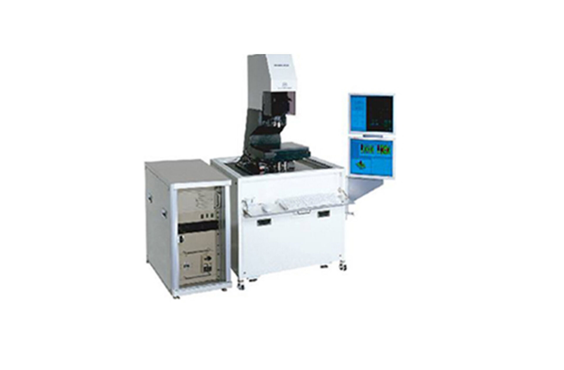
Research and analysis equipment utilizing the principle of non-contact 3D surface measurement
Non-contact 3D surface measurement
Nanometer-level resolution

High technology
- Non-contact 3D surface profilometry
- Nanoscale resolution

Application
- 3D step height, thin film thickness, and CD measurement of micro-pattern